NEWS
Updated 13/07/2015
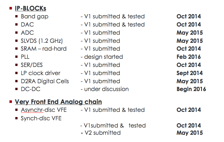
- Here the list of IP-blocks and Very Front End designed by the CHIPIX65 project.
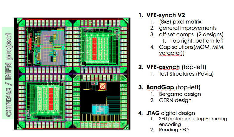
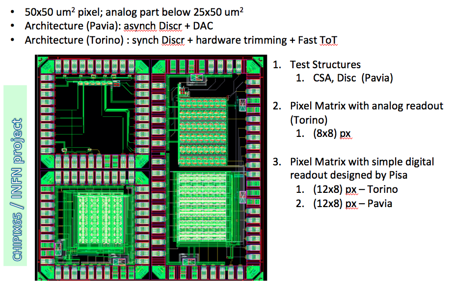
- Chip die with Very-Front End analog chain: 8x8 pixel array with analog output; 16x8 pixel array with sinple digital readout; test-structures for part of analog chain
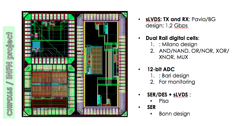
- Chip die with several IP-blocks: sLVDS (TX,RX), Digital cells radiation hard by design using a Dual Rail methodology; a 12-bit ADC; SER/DES (for 3 Gbps) + sLVDS cell.
- Chip die with Very-Front End analog chain: 8x8 pixel array with analog output; 16x8 pixel array with sinple digital readout; test-structures for part of analog chain
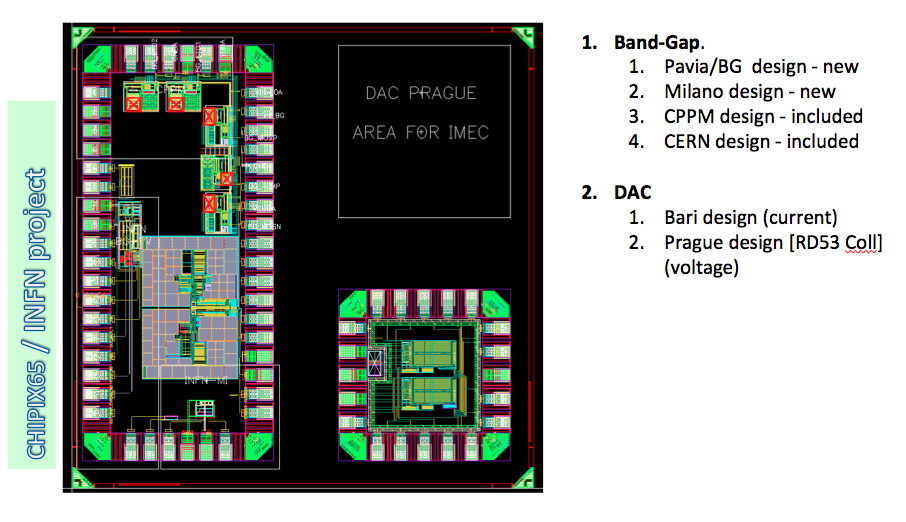
- Chip die with IP-block: 10-bit DAC in current; Band-Gap;
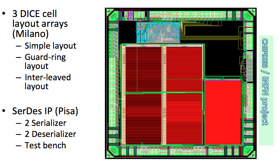
- Chip die with IP-block: Dice-SRAM DAC; SER/DES;
YEAR 2015
-
In the first half of year 2015, the CHIPIX65 project has sent new CMOS 65nm design of prototypes
for IP blocks and for the second version of small matrixes of pixels dedicated to the study analog
very front end architectures. The prototypes have been submitted in May 2015 as two different dices of 2x2.
Right now the activity of CHIPIX65 is focused on the design of a small pixel matrix of 64x64 pixels, with a first version of a realistic digital architecture for the HL_LHC. The chip will be design using a Digital-on-Top methodology.
May 2015 submission: CHIPIX-VFE-2
May 2015 submission: CHIPIX-IP-3
YEAR 2014
-
In the year 2014, the CHIPIX65 project has designed the first CMOS 65nm design of prototypes
for the first IP blocks and for the first small matrixes of pixels dedicated to the study analog
very front end architectures. The prototypes have been submitted in October 2014 as three different dices of 2x2
mm2 to the foundry and are now under test in the different groups.
October 2014 submission: CHIPIX-VFE-1
October 2014 submission: CHIPIX-BIAS-1
October 2014 submission: CHIPIX-SRAM-1